Third generation wide band gap semiconductor materials silicon carbide (SiC) and gallium nitride (GaN)
In the development process of the semiconductor industry
Release time:
2019-02-23
Source:
In the development process of the semiconductor industry, people usually call Si and Ge element semiconductors as first-generation electronic materials, compound semiconductors such as GaAs, InP, and InAs as second-generation semiconductor materials, and group III nitrides (mainly including GaN, related compounds InN, AIN and its alloys), wide-gap compound semiconductors such as SiC, InSe, and diamond are called third-generation semiconductor materials.

Figure 1: Semiconductor
Semiconductor is a material between conductor and insulator. Semiconductor technology is indispensable in all aspects of our lives. Electrical appliances, lighting, mobile phones, computers, electronic equipment, etc. all require semiconductor materials. The third generation of semiconductor materials has developed well. The ones are silicon carbide (SiC) and gallium nitride (GaN), of which silicon carbide developed earlier.
硅 Silicon carbide crystal structure has the characteristics of homogeneous polytype, and its basic structure is Si-C tetrahedron structure. It consists of a tetrahedron formed by four Si atoms surrounded by a carbon atom. In the same way, a Si atom is also surrounded by a tetrahedron of four carbon atoms, which belongs to a close-packed structure.
Gadolinium gallium nitride is a compound of nitrogen and gallium, which is a semiconductor with a direct energy gap. The compound has a structure similar to wurtzite and has a high hardness. GaN has a wide energy gap of 3.4 electron volts and can be used in high-power, high-speed optoelectronic components.
Let's see what is the difference between the key characteristics of gallium nitride and silicon carbide.

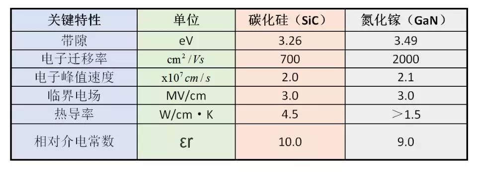
Comparison of key characteristics of silicon carbide and gallium nitride:
As can be seen from the table above, GaN provides high electron mobility, excellent breakdown capability, higher electron density and speed.
Although the performance of gallium nitride is better, there are still problems in development
The rapid development of gallium nitride (GaN) semiconductor materials and devices has now become a dazzling star in wide band gap semiconductor materials, but the development of gallium nitride materials still has problems to be solved: First, how to obtain high-quality, large-sized GaN The seed crystal, because it takes several years to directly cultivate a two-inch seed crystal by the ammonia method; the second is that the gallium nitride industry chain has not been fully formed.
In comparison, silicon carbide has become more mature in the current wide band gap semiconductor materials, and has formed a global material, device and application industry chain. In the third-generation semiconductor materials, both have very broad application prospects.
Application fields of third-generation wide-bandgap semiconductors
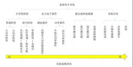
The third generation of wide-bandgap semiconductors can be applied to semiconductor lighting, power electronics, lasers and detectors, and four other fields (see Figure 3 below). The maturity of the industry is different in each field. In the forefront of research, wide band gap semiconductors are still in the laboratory research and
developme
nt stage.

Figure 2: Application fields of third-generation wide band gap semiconductor materials
Development status of third-generation semiconductors
At present, the United States, Japan, and Europe have absolute say in third-generation semiconductor technology. Compared with the United States and Japan, China started late in the third generation of semiconductor materials, with a lower level. With the country's emphasis on the third-generation semiconductor materials, in recent years, China's semiconductor material market has developed rapidly. Among them, silicon carbide and gallium nitride-based materials have attracted much attention. In 2016, China initiated the organization and implementation of the key special projects of the “strategic advanced electronic materials” of the “13th Five-Year Plan” national key research and development plan. Level of focus support.
The third-generation semiconductor technology is gradually upgraded, the market is gradually opened, policies are fully accelerated, capital is actively entered, and enterprises are expedited. The third-generation semiconductor industry in China has ushered in the first year of development.
national,semiconductor


